BNC E-news: Week of November 15th, 2021

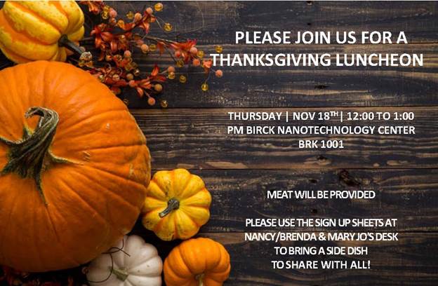
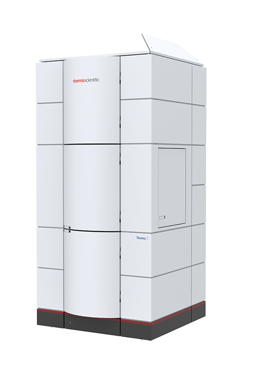
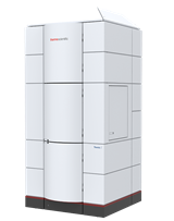
[cid:image006.png@01D7401C.A3F567B0] Seminars /Workshops / Events BNC Faculty Seminar Series Brett Savoie Charles Davidson Assistant Professor of Chemical Engineering (by courtesy) at Purdue University Thursday November 18th, 2021 12:00pm – 1:00pm, Zoom https://purdue-edu.zoom.us/j/98695180597 Topic : How Things Fall Apart: Learning from Degradation Chemistry Seminar for Neurotrauma and Diseases<https://vet.purdue.edu/cpr/Seminar%20for%20Neurotrauma.php> Sponsored by Plexon Neurotechnology Systems Wednesdays | 4-5pm | via Zoom NanoHub Workshop Announcement nanoHUB is excited to announce that a new workshop has been scheduled in the Fall 2021 session of our Hands-on Data Science and Machine Learning Training Series. Series information: Our series is aimed at active researchers and educators and designed to introduce practical skills with online, hands-on activities that participants will be able to incorporate in their own work. Hands-on activities will use nanoHUB cloud computing resources, negating the need to download or install any software. All that is required of the audience is an internet connection and an hour to spare for the demonstration. After the training sessions, you will be able to continue using nanoHUB for research or education. Recordings and associated materials from prior workshops can be found at the workshop webpage: https://nanohub.org/groups/ml/handsontraining<https://click.mail.nanohub.org/?qs=fa5d19fdba110be3328ac7c0e6aa1c23ed02fcba3677ed0156b8cb3c81979933cbdb68e347e60b1f0c742b032dda0b2b6801b71140bc86b33aa0ebe512e85b1d> Register soon as seats are limited. Date/Time: Wednesday, November 17, 2021 / 1:00 PM – 2:00 PM EST Title: Integrating Machine Learning with a Genetic Algorithm for Materials Exploration Presenter: Joe D. Kern, Georgia Institute of Technology, Ramprasad Group Register for this workshop here<https://click.mail.nanohub.org/?qs=fa5d19fdba110be31df082c3e47a7f7022739f4c0c0d7e1a4c5fbc845fddb32d0043e5d90d2aac11e1e7121eba99c6f6e9386249d725206fe3a96af954f6a60a> Abstract: The genetic algorithm is a computer algorithm inspired by nature: selecting parents of a generation via some fitness function, crossing-over the parent genes (reproduction), and randomly mutating the genes of the children. In this talk, we will explore how this algorithm can be used for materials discovery by: 1. Generating swift material property prediction using machine learning (ML) 2. Creating an algorithm to design new materials from combinations of prior ones 3. Integrating the ML property predictors with the design algorithm to discover new materials PolyGA, an implementation of the genetic algorithm for the polymer domain, will be used as the basis for this exploration. Bio: Joe D Kern is a Materials Science and Engineering graduate student at the Georgia Institute of Technology in the Ramprasad Group. Prior to graduate school, he dual majored in Materials Science and Computer Science at the University of Wisconsin – Madison and spent six years in the Minnesota National Guard as an Arabic Linguist. His research involves utilizing computational techniques, such as genetic algorithms and machine learning, to expedite materials discovery in the polymer chemical space. Regards, Alejandro Strachan Deputy Director, nanoHUB Arun Mannodi Kanakkithodi (he/him/his) Assistant Professor, School of Materials Engineering, Purdue University https://www.mannodigroup.com/ 2021 Birck Nanotechnology Center Research Image Contest Sponsored by NSAC and Birck leadership - $600 in prize awards for student entries Please share your research images which showcase the beauty you’ve observed around you at Birck! All members of the Birck community – students, staff, and faculty – are welcome to submit their images that can include not only research images but also photos of life here at Birck. For research images, we ask that you also write a short paragraph explaining what we are looking at and why it is significant to you. We will assemble a panel of judges and announce awards at the BNC Holiday Party in December, and student entries are eligible to win: $300 for 1st place $200 for 2nd place $100 for 3rd place You can submit multiple images anytime between now and November 30, 2021 to a new MS Teams channel we have set up for the image contest, see link below: https://teams.microsoft.com/l/channel/19%3abf8be291dbb9468b831b6e0de523b930%... If you have issues or questions, please email Neil Dilley at ndilley@purdue.edu<mailto:ndilley@purdue.edu> . Happy image hunting! [Text, logo, company name Description automatically generated] and the Birck Nanotechnology Center [A picture containing text, indoor, seat Description automatically generated][A picture containing background pattern Description automatically generated][A group of colorful feathers Description automatically generated with low confidence][A picture containing indoor, birthday, office, chocolate Description automatically generated][A picture containing tool Description automatically generated][cid:image015.png@01D7BEA6.8D0C2170][A close-up of a person's chest Description automatically generated with medium confidence] Birck Events<https://www.purdue.edu/discoverypark/birck/events/index.php> and Birck News<https://www.purdue.edu/discoverypark/birck/news/index.php> Thanksgiving Luncheon (BNC Staff only) [cid:image013.jpg@01D7D7C9.B402CE00] JOB POSTINGS: R&D Senior Design Engineer at Alpha & Omega Semiconductor Alpha & Omega Semiconductor is looking for a Senior Design Engineer who will work in a dynamic team environment at AOS headquarter located in Sunnyvale, CA. The main responsibility of this position is to work with marketing/process integration/product engineering group to develop silicon power device technology. Application link: Senior Design Engineer - Sunnyvale, CA - Alpha & Omega Semiconductor Jobs (applicantpro.com)<https://caosmd.applicantpro.com/jobs/2050960.html> R&D Senior Process Integration Engineer at Alpha & Omega Semiconductor Alpha & Omega Semiconductor is looking for a Senior Process Integration Engineer who will work in a dynamic team environment at AOS Semiconductor's leading technology fabrication facility (Jireh Semiconductor) located in Hillsboro, Oregon. The focus of this position is to work with device/process module/product engineering group to develop silicon power device process technology and improve existing technology yield. Primary responsibilities are to process flow implementation, electrical characterization (failure analysis), and wafer level testing yield monitoring. Application link: Entry Level MS or PHD Process Integration R&D Engineer - Hillsboro, OR - Jireh Semiconductor Jobs (applicantpro.com)<https://aosmd.applicantpro.com/jobs/1949301.html> Opening in OxideMEMS lab Sunil Bhave’s OxideMEMS Lab <https://engineering.purdue.edu/oxidemems/publications.html> explores inter-domain coupling in Opto-mechanical, Spin-Acoustic and Atom-MEMS devices. PhD, Postdoctoral and Research Associate positions are available in these areas: · Superconducting qubit and cryo-CMOS circuits · Resonators and switches · MEMS-engine for LIDAR · Piezo-on-nitride transducers for atom-mechanics Expertise in many and most of Microfabrication, PiezoMEMS, Photonics, Quantum Mechanics, Microwave circuits, PCB design, ADS/HFSS, Comsol, Python and Labview is required. Please send CV to bhave@purdue.edu<mailto:bhave@purdue.edu> if you are interested.link<http://interested.link> [cid:image020.png@01D7BEAF.D3C3AE90] Postdoctoral Position – Nonlinear Nanophotonics – Deadline Nov.15, 2021 Fliers with more information posted on the bulletin boards. An electronics engineer position is available in the Smart Sensing and Electronics Systems Branch of NASA, located at the Glenn Research Center (GRC). The focus of the successful candidate will be on research, design, development, simulation and testing of sensing devices, transducers, components, and related circuitry for application to aerospace research and development endeavors. See https://www.usajobs.gov/GetJob/ViewDetails/615488500 for details. Contact Dallas Morisette morisett@purdue.edu<mailto:morisett@purdue.edu> for more detail Nanofabrication Engineer at Microsoft Microsoft Azure Quantum at Station Q Purdue seeks a nanofabrication engineer in the device fabrication group. You will join a multi-disciplinary team of theoretical and experimental physicists, materials scientists, and hardware and software engineers working at the forefront of quantum computing. You should have experience in device fabrication and characterization techniques. Our work at Station Q Purdue in West Lafayette, Indiana is part of global Microsoft Quantum research effort in topological quantum computing. Responsibilities: Responsibilities include develop, operate, and characterize semiconductor device fabrication processes in the Birck Nanotechnology Center cleanroom facilities located at Purdue University. Accurately documenting and effectively communicating all procedures and results to the larger research group is an essential aspect of the position. The candidate may also be required to assist in the maintenance of equipment. Qualifications: A successful candidate must have: • • Master’s degree in Physics, Materials Science or Electrical Engineering. Other engineering disciplines will also be considered. • • Hands-on experience working with some or all of the following semiconductor process areas: lithography, thin film deposition and etch. • • Ability to follow protocols to operate sophisticated experimental equipment and to safely work with industrial solvents, acids, and bases in a cleanroom environment • • Excellent written and oral communication skills. • • Proficiency at accurately documenting processes and protocols. • • Strong attention to detail and good organizational skills. • • Strong desire to work in a collaborative international team. Preference may be given to candidates with the following additional qualifications: • • Industry experience in semiconductor device process integration. • • Expertise in thin film characterization, both structural and electrical. • • Familiarity with design and layout tools for chip scale devices. Please send your resume to flgriggi@microsoft.com<mailto:flgriggi@microsoft.com>, selected candidates will be contacted for interviews. NSAC Fab Forum There will be no NSAC Fab Forum this Tuesday NSAC Coffee Hour There will be no NSAC Coffee Hour this Friday Birck Nanotechnology Center Advanced Capabilities Themis Z Aberration Corrected STEM/TEM [cid:image017.png@01D7DA28.14657760]Features: * Atomic resolution down to 65 pm in both TEM and STEM mode as the column contains a probe and image corrector * Monochromatic gun + EELS spectrometer, which combine deliver an energy resolution of 120 meV at 80kV – great for plasmons and oxidation state studies * SuperX EDX detector, high signal to n oise ration due to a 4-quadrant detector set up * Flexible high tension range: 300, 200, 80, 60kV. Lower kVs are ideal for electron-beam sensitive samples Contact: Rosa E Diaz– rdiazri@purdue.edu<mailto:rdiazri@purdue.edu> (Staff in Charge), BRK 1269A ***To post an announcement in the weekly BNC E-news please send to Sangeeta Abrol @ abrols@purdue.edu***<mailto:abrols@purdue.edu***> Follow us on Facebook and Twitter [Facebook icon]<https://www.facebook.com/nano.purdue.edu/> [Twitter icon] <https://twitter.com/BNCPurdue>
participants (1)
-
 Abrol, Sangeeta Saddul