BNC E-news: Week of August 9th, 2021

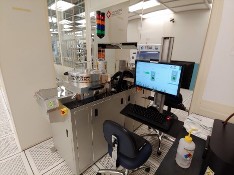
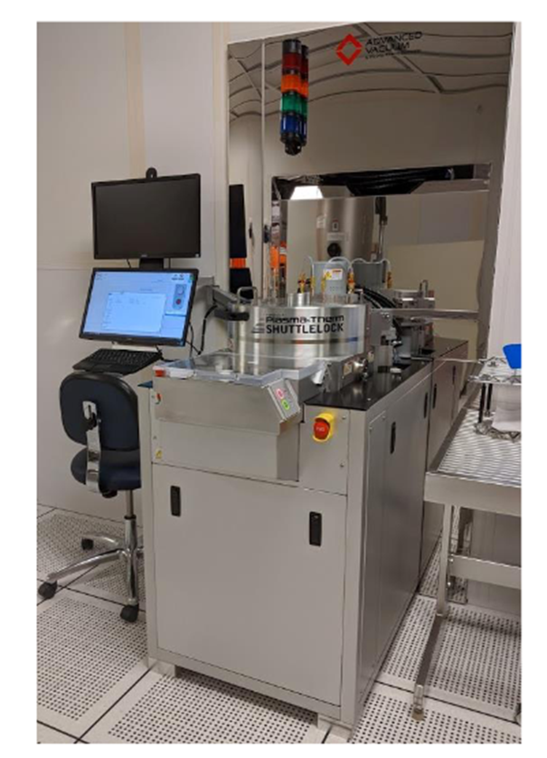
[cid:image006.jpg@01D685C3.FA345960] Seminars /Workshops / Events nanoHUB is excited to announce that a new workshop has been scheduled in the Summer 2021 session of our Hands-on Data Science and Machine Learning Training Series. Series information: Our series is aimed at active researchers and educators and designed to introduce practical skills with online, hands-on activities that participants will be able to incorporate in their own work. Hands-on activities will use nanoHUB cloud computing resources, negating the need to download or install any software. All that is required of the audience is an internet connection and an hour to spare for the demonstration. After the training sessions, you will be able to continue using nanoHUB for research or education. Register soon as seats are limited. Date/Time: Wednesday, August 11, 2021 / 1:30 PM - 2:30 PM EDT Title: Debugging Neural Networks Presenter: Rishi Gurnani, a PhD student at Georgia Tech in Professor Rampi Ramprasad's Group Register for this workshop here<https://click.mail.nanohub.org/?qs=840f0f66ba4b18e6078d9ea75e985292ba17c5d207180c0932c3dc05002cc5f1891675e6104d6aa6821ee6f20fcb19b8dc8e4a3633710455> Abstract: Imagine a program that did not pass along helpful descriptions of errors, let alone provide a notification that an error has occurred. How would one even begin to debug such a nightmare? Error-laden deep learning systems are susceptible to such "silent failures". The reason for silent failure in deep learning is that any code representing a mathematically valid expression will fly, even if the coded expression is not mathematically logical. Further, the capacity of a deep learning model may be large enough to compensate for illogical code. Thus, the performance of the model may look reasonable enough that one does not re-examine the code for errors. To mitigate chances of falling into this trap, we have collected and encoded a list of common-sense checks that deep learning systems should pass. Several checks are borrowed from a well-written blog post1 by Andrej Karpathy, Tesla's Director of Artificial Intelligence, while some are original. The implementation of these checks is original work and is known as NetDebugger. Failure of any check results in an error along with a helpful error message. The presentation will start with an overview of deep learning theory to motivate the logic in NetDebugger and end with a hands-on NetDebugger tutorial involving PyTorch, RDKit, and polymer data (made publicly available by the Ramprasad Group at https://khazana.gatech.edu/ ). NetDebugger has saved me time in my research and, I hope, will be useful to the community. 1Karpathy A., A Recipe for Training Neural Networks, http://karpathy.github.io/2019/04/25/recipe/ Bio: Rishi Gurnani is currently a PhD student in the Ramprasad Group at Georgia Tech and a Masters Student in Computer Science at Georgia Tech. Rishi is also the Technology Development co-Lead at Matmerize, a polymer informatics start-up. His research focuses on the intersection of polymer science and machine learning. Previously, he received his Bachelor of Science in Materials Science and Engineering from the University of California, Berkeley. BNC Faculty Seminar Series (will resume fall semester, 2021) Previous Talks: https://engineering.purdue.edu/Intranet/Groups/BNC/FacultySeminars Birck Events<https://www.purdue.edu/discoverypark/birck/events/index.php> and Birck News<https://www.purdue.edu/discoverypark/birck/news/index.php> Birck Nanotechnology Center Advanced Capabilities [cid:image004.png@01D78D29.5CB5E8C0]Plasma-Therm Apex ICP RIE Etcher<https://wiki.itap.purdue.edu/display/BNCWiki/Plasma-Therm+Apex+SLR> * ICP Power up to 2,000W and Bias Power up to 600W * Configured with 10 Process Gasses * Chamber and Chuck Temperatures up to 60C Other Capabilities: Has End Point Detection capabilities with a laser-based system which measures the laser signal reflected from a target location on the substrate surface. Location: BRK Cleanroom Bay K Contact: Francis Manfred (fmanfred@purdue.edu<mailto:fmanfred@purdue.edu>) Please visit the Birck Wiki<https://wiki.itap.purdue.edu/display/BNCWiki/> to learn about the wide array of fabrication and characterization equipment at the facility Opening in OxideMEMS lab Sunil Bhave's OxideMEMS Lab <https://engineering.purdue.edu/oxidemems/publications.html> explores inter-domain coupling in Opto-mechanical, Spin-Acoustic and Atom-MEMS devices. PhD, Postdoctoral and Research Associate positions are available in these areas: * Superconducting qubit and cryo-CMOS circuits * Resonators and switches * MEMS-engine for LIDAR * Piezo-on-nitride transducers for atom-mechanics Expertise in many and most of Microfabrication, PiezoMEMS, Photonics, Quantum Mechanics, Microwave circuits, PCB design, ADS/HFSS, Comsol, Python and Labview is required. Please send CV to bhave@purdue.edu<mailto:bhave@purdue.edu> if you are interested.link<http://interested.link> Kepler Computing Process Engineer Opening Job Category: R&D Primary Location: West Lafayette, IN and Berkeley, CA, USA Job Title: Process Engineer Job Description: Kepler Computing is building fundamentally new blocks to accelerate computation beyond Moore's law. The founding team consists of industry veterans spanning across the full compute stack of product, architecture, circuit, device, manufacturing and physics. Materials and process development are an integral part of Kepler Computing. In this highly visible role of a Process Engineer, you'll join a team helping to develop the most efficient means for device processing, enabling computing systems to do more with less energy. Process Engineers take responsibility for specifying and developing dry etch solutions for various thin film stacks or mono-layers, as well as assist with ongoing efforts to integrate new etch solutions into our integrated device process flows. You will take a demanding set of functions and turn them into the computing technology that transforms how the world works, plays, learns and communicates. If you are looking for a position where you can see the end results of your work making a real impact on the tech world and on real experiences, this is the position for you. The candidate must execute projects based tasks that include process development, integration and metrology/characterization of materials working side-by-side with a diverse group of engineers to solve problems creatively with deadlines; assume ownership and accountability for successful completion of projects and programs; report results both internally and externally with presentation and formal report packages; interact with other engineers in areas of design, growth, fabrication and test to facilitate fabrication and device optimization; metrology and defectivity experience and process development stablished within coupon line, 100mm, 150mm and 300mm fabrication line. This position will initially be situated in West Lafayette, IN for about the first 3 months. The candidate will need to perform R&D work at Purdue University's Birck Nanotechnology Center. After the initial period as mentioned above, the candidate will need to relocate to Berkely, CA. The candidate is expected to have good oral and written communication skills and experience in technical writing. Equipment that will be used during the course of performing essential functions include RIE and IBE etch tools, SEM, AFM and other analytical instrumentation and some physical tasks may require standing and walking, lifting objects up to 20 pounds, and the use of hand tools. Full description and how to apply attached. Follow us on Facebook and Twitter [Facebook icon]<https://www.facebook.com/nano.purdue.edu/> [Twitter icon] <https://twitter.com/BNCPurdue> Jaime Turner Lead Administrative Assistant to the Director | Birck Nanotechnology Center BRK | 1205 W State Street | West Lafayette, IN 47907 o: 765-494-3509<tel:7654943509> | m: 765-491-3064<tel:7654913064> | jjturner@purdue.edu<mailto:jjturner@purdue.edu> [83324AA6]<https://www.purdue.edu/>
participants (1)
-
 Turner, Jaime J