
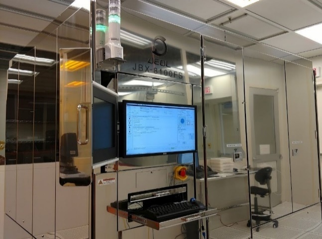
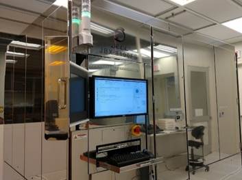
[cid:image006.png@01D7401C.A3F567B0] Seminars /Workshops / Events/Announcement Workshop Quantum Programming Workshop for Purdue Women Engineers and Scientists Date & time: Feb 25th 2022, 11:59 AM to 4:00 PM In-Person Location: Neil Armstrong Hall of Engineering Room 2008 (Virtual attendees can use Zoom) Open registration: https://purdue.ca1.qualtrics.com/jfe/form/SV_3yifGFEsUYmUX8q Learning from the history of the digital revolution in which women played a significant role in driving software development in the early days, the IQPARC project is paying particular attention to attracting women scientists and engineers from different disciplines at Purdue. IQPARC is holding a half-day hands-on hybrid workshop (lunch provided for in-person attendees at 11:30 am) for women engineers and scientists at Purdue. The workshop features webinars by Industry leaders, e.g., Microsoft, IonQ, and Quantum Computing Inc., and Purdue's Professors and students on the following topics: * Introduction to IQPARC (10min) Prof. Mahdi Hosseini (Purdue ECE) * Introduction to IonQ quantum processors (50min) Sarah Kreikemeier, Senior Mechanical Engineer, IonQ Inc. (NYSE: IONQ) * Cloud quantum programming, Microsoft Azure Quantum (120min) Mariia Mykhailova, Principal Software Engineer at Microsoft Quantum * Solving optimization problems with quantum computers, Quantum Computing Inc.(50min) QCi Presenter: TBA * Cloud quantum programming using IBM Qiskit language (50min) Purdue student presenter: Ganga Jayarathna, recorded video will be available on IQPARC.com after the workshop All attendees will receive a certificate of competition from IQPARC. Moreover, attendees will have opportunities to participate in follow-up programming events (with free access to quantum computers) and apply for awards and summer scholarships offered by IQPARC. To learn more about the Center for Innovation in Quantum Pedagogy, Application and its Relation to Culture (IQ-PARC), please visit the home page at https://www.iqparc.com Questions can be directed to: lidongyang@purdue.edu<mailto:lidongyang@purdue.edu> This effort is supported by the National Defense Education Program (NDEP-STEM) under Grant No. HQ0034-21-1-0014 [cid:image007.jpg@01D81133.C6F37D40] Announcement Mask Protocols in the Cleanroom We have observed various masking practices in the cleanroom recently so as a reminder for those using our Birck cleanroom, please continue to follow our COVID mask protocols. Masking requirements are either to use an M3 N95 mask by itself or use a standard mask under the cleanroom veil. If you have any questions please contact a staff member. Thanks, Ron Birck Engineering New Employee We are pleased to welcome Michelle Radke to the Birck team as our New Logistic Coordinator. Michelle will be joining us starting on 1/31/2022. Mark Voorhis Building Manager Birck Events<https://www.purdue.edu/discoverypark/birck/events/index.php> and Birck News<https://www.purdue.edu/discoverypark/birck/news/index.php> JOB POSTINGS: R&D Senior Design Engineer at Alpha & Omega Semiconductor Alpha & Omega Semiconductor is looking for a Senior Design Engineer who will work in a dynamic team environment at AOS headquarter located in Sunnyvale, CA. The main responsibility of this position is to work with marketing/process integration/product engineering group to develop silicon power device technology. Application link: Senior Design Engineer - Sunnyvale, CA - Alpha & Omega Semiconductor Jobs (applicantpro.com)<https://caosmd.applicantpro.com/jobs/2050960.html> R&D Senior Process Integration Engineer at Alpha & Omega Semiconductor Alpha & Omega Semiconductor is looking for a Senior Process Integration Engineer who will work in a dynamic team environment at AOS Semiconductor's leading technology fabrication facility (Jireh Semiconductor) located in Hillsboro, Oregon. The focus of this position is to work with device/process module/product engineering group to develop silicon power device process technology and improve existing technology yield. Primary responsibilities are to process flow implementation, electrical characterization (failure analysis), and wafer level testing yield monitoring. Application link: Entry Level MS or PHD Process Integration R&D Engineer - Hillsboro, OR - Jireh Semiconductor Jobs (applicantpro.com)<https://aosmd.applicantpro.com/jobs/1949301.html> Opening in OxideMEMS lab Sunil Bhave's OxideMEMS Lab <https://engineering.purdue.edu/oxidemems/publications.html> explores inter-domain coupling in Opto-mechanical, Spin-Acoustic and Atom-MEMS devices. PhD, Postdoctoral and Research Associate positions are available in these areas: * Superconducting qubit and cryo-CMOS circuits * Resonators and switches * MEMS-engine for LIDAR * Piezo-on-nitride transducers for atom-mechanics Expertise in many and most of Microfabrication, PiezoMEMS, Photonics, Quantum Mechanics, Microwave circuits, PCB design, ADS/HFSS, Comsol, Python and Labview is required. Please send CV to bhave@purdue.edu<mailto:bhave@purdue.edu> if you are interested link<http://interested.link> Nanofabrication Contractor Engineer for Microsoft Quantum Microsoft Azure Quantum at Station Q Purdue seeks a nanofabrication engineer in the device fabrication group. You will join a multi-disciplinary team of theoretical and experimental physicists, materials scientists, and hardware and software engineers working at the forefront of quantum computing. You should have experience in device fabrication and characterization techniques. Our work at Station Q Purdue in West Lafayette, Indiana is part of global Microsoft Quantum research effort in topological quantum computing. Responsibilities: Responsibilities include develop, operate, and characterize semiconductor device fabrication processes in the Birck Nanotechnology Center cleanroom facilities located at Purdue University. Accurately documenting and effectively communicating all procedures and results to the larger research group is an essential aspect of the position. The candidate may also be required to assist in the maintenance of equipment. Qualifications: A successful candidate must have: * * Master's degree in Physics, Materials Science or Electrical Engineering. Other engineering disciplines will also be considered. * * Hands-on experience working with some or all of the following semiconductor process areas: lithography, thin film deposition and etch. * * Ability to follow protocols to operate sophisticated experimental equipment and to safely work with industrial solvents, acids, and bases in a cleanroom environment * * Excellent written and oral communication skills. * * Proficiency at accurately documenting processes and protocols. * * Strong attention to detail and good organizational skills. * * Strong desire to work in a collaborative international team. Preference may be given to candidates with the following additional qualifications: * * Industry experience in semiconductor device process integration. * * Expertise in thin film characterization, both structural and electrical. * * Familiarity with design and layout tools for chip scale devices. Please send your resume to flgriggi@microsoft.com<mailto:flgriggi@microsoft.com>, selected candidates will be contacted for interviews. Graduate Research Assistantship Opportunity: Deposited Gate Oxides for SiC MOSFETs Up to two graduate research assistantships are available in the area of silicon carbide metal-oxide-semiconductor (MOS) devices. SiC is a wide bandgap semiconductor with a high critical field, making it an exciting material for power electronic devices. SiC MOSFETs are now commercially available, but do not yet achieve their full potential. Our group is approaching this problem from several directions, including a new device trench MOSFET geometries inspired by modern FinFETs and alternative gate insulator fabrication methods. Research activities will include fabrication and characterization of SiC MOS capacitors and MOSFETs with gate oxides formed by thermal oxidation, atomic layer deposition (ALD), and other methods. The student will gain a detailed understanding of the physics of the MOS interface and will learn various methods of characterizing devices, including MOS CV analysis, interface state density and carrier mobility. For more information or to apply, send resume and contact information to: Dallas Morisette Research Assistant Professor morisett@purdue.edu<mailto:morisett@purdue.edu> [cid:image014.png@01D81133.C6F37D40] Department of Health and Human Services National Institutes of Health Postdoctoral Fellow Position in the NIBIB's Section on Mechanobiology Fields: Mechanobiology, Biophysics, Engineering, High-resolution Imaging, Cell Biology, Developmental Biology Research Project Title: Mechanobiology of Self-Organization in Cancer Project Description: The NIBIB's Section on Mechanobiology (https://www.nibib.nih.gov/labs-at-nibib/section-mechanobiology) at the National Institutes of Health is recruiting a Staff Scientist. The focus of the Cartagena-Rivera lab the development and use of advanced Atomic Force Microscopy (AFM) tools for cellular and tissue mechanics investigation. We seek to understand several important biological processes by applying physics and engineering principles, particularly: the molecular-mechanical regulation of the actomyosin cortex and glycocalyx of highly malignant cancers (including melanoma, breast, ovarian, and pancreatic); the structural-molecular-mechanical regulation of the solid tumor microenvironment for deciphering self-organization, morphogenesis, and growth in cancer biology; and the anisotropic mechanical properties of developmental and mature inner ear sensory and non-sensory epithelial tissues using a novel noncontact AFM approach. This position will work at the intersection of biophysics, engineering, mathematics, and molecular/cellular/developmental biology to study the mechanobiological regulation of cells and tissues during development and disease. Furthermore, will work on development of new Atomic Force Microscopy-based technologies to study fast multiparametric and multidimensional cellular and tissue processes, advances the state of the art AFM imaging methods for high spati-temporal and quantitative nanomechanical mapping. In addition, will work closely with collaborating cell biologist, geneticists, engineers, and byophysists within and outside the NIH. Qualifications: The candidate must have a Ph.D. degree in cellular biology, biophysics, biomedical or mechanical engineering, or related discipline, with some background in molecular cell biology and developmental biology. The candidate must demonstrate ability to work in a multidisciplinary and diverse team. We are seeking a highly motivated individual who has a demonstrated record of productivity and success in scientific and engineering projects. The candidate must have experience on cellular and tissue mechanics, tissue culture, AFM imaging, high-resolution optical imaging, and programming for data analysis (preferably Julia, Python, MATLAB, or R) and/or experimental devices control (preferably LabVIEW). Position Location: Bethesda, Maryland (NIH main campus) To Apply: Salary is determined by the NIH stipend level for Post-Doctoral Trainees and Fellows.Applicants are invited to submit a curriculum vitae including a list of publications, a maximum one-page summary of research interests, and names and contact details of three referees to Dr. Cartagena-Rivera by email at alexander.cartagena-rivera@nih.gov. The National Institutes of Health is an equal opportunity employer. The NIH is dedicated to building a diverse community in its training and employment programs. For more information or to apply, send resume and contact information to: Daniel M. Suter, PhD Professor Department of Biological Sciences Purdue University 915 West State Street West Lafayette, IN 47906 dsuter@purdue.edu<mailto:dsuter@purdue.edu> NSAC Fab Forum NSAC Fab Forum every Tuesday 2:00pm-2.30pm NSAC Coffee Hour NSAC Fab Forum every Friday 2:00pm-2.30pm Birck Nanotechnology Center Advanced Capabilities JEOL-8100 FS Electron Beam Lithography [cid:image020.png@01D81133.C6F37D40][JEOL8100FS.jpg] Features: * Fast 125MHz Scanning * Two writing modes -ultra fine and high throughput * Stitching of +/- 9 nm in ultra-fine writing and +/- 20 nm in high throughput * Can write on small substrates up to 200 mm substrates * GenISys BEAMER software used for data fracturing Location: BRK Cleanroom P Bay Contact: Rill Rowe (wrowe@purdue.edu) or Dr. Justin Wirth (jcwirth@purdue.edu) Please visit the Birck Wiki to learn about the wide array of fabrication and characterization equipment at the facility<https://wiki.itap.purdue.edu/display/BNCWiki/> ***To post an announcement in the weekly BNC E-news please send to Sangeeta Abrol @ abrols@purdue.edu***<mailto:abrols@purdue.edu***> Follow us on Facebook and Twitter [Facebook icon]<https://www.facebook.com/nano.purdue.edu/> [Twitter icon] <https://twitter.com/BNCPurdue>